


Applications:
- Alignment - Wafer flat and notch aligners are used in the semiconductor industry to ensure that wafers are oriented correctly during various processes, such as lithography, deposition, and etching. The flat aligner has a notch or flat that corresponds to the orientation of the wafer's crystal lattice structure. This is critical because the orientation of the wafer affects the performance and functionality of the final semiconductor device.
- Lot integrity - Aligners are also used in the semiconductor industry to aid operators in performing lot integrity checks. By rotating the wafer scribe, which is the identification marking on the wafer's edge, to be visible to the operator, the operator can verify that the correct lot of wafers is being loaded into a production tool. This is an important step in preventing errors and ensuring consistent product quality.
- Edge inspection - Wafer flat and notch aligners are also used in the semiconductor industry to inspect wafers for edge defects. This macro inspection procedure is usually done under a light source and involves examining the edges of the wafer for any chips, cracks, or other imperfections. This is an important step in preventing wafer breakage during subsequent processing steps, as edge defects can weaken the wafer and cause it to break or fail. By using wafer flat and notch aligners to identify and inspect these defects, operators can take steps to prevent further processing of defective wafers and avoid costly production delays.
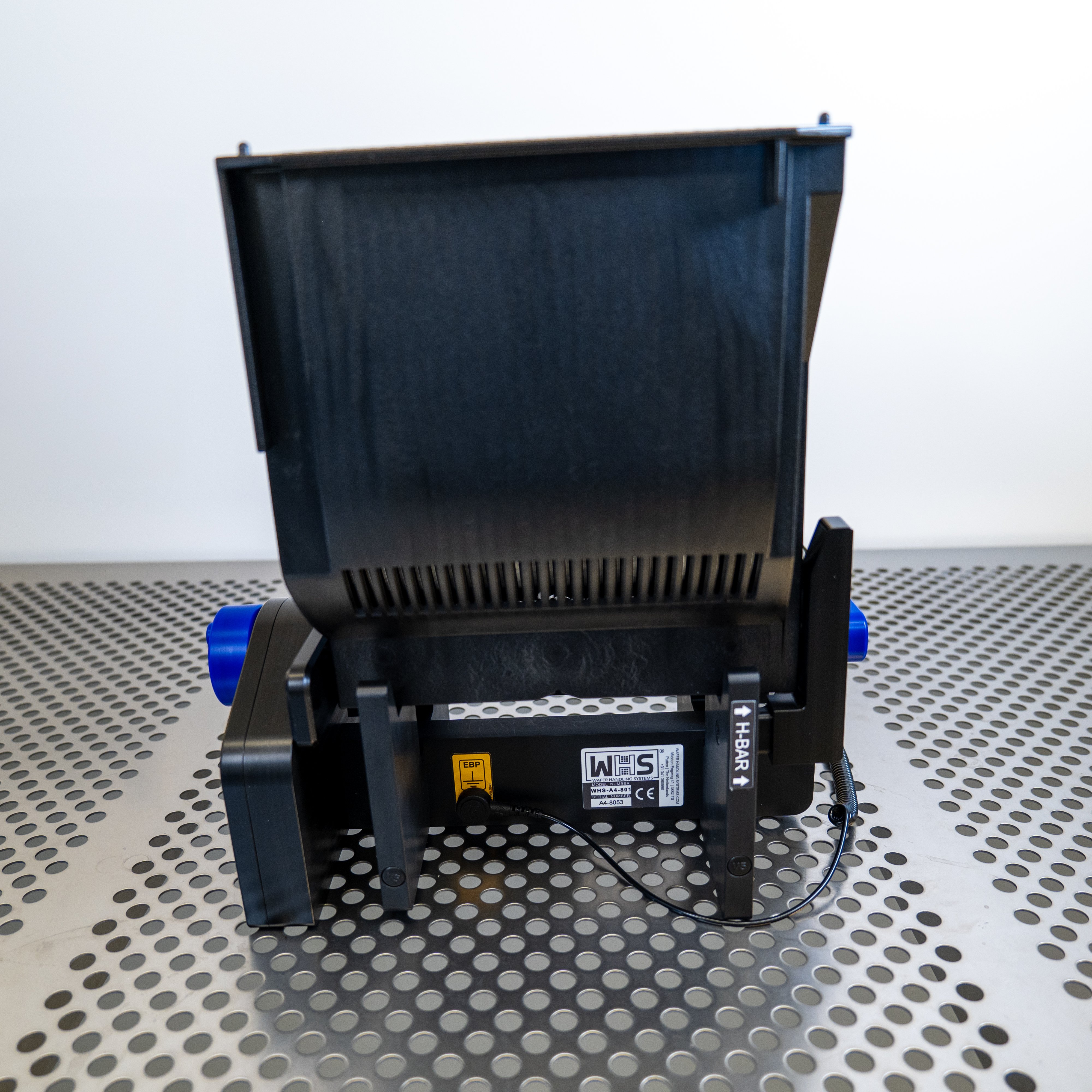
The WHS-A4 series is a precision manual wafer notch aligner designed for top and bottom bulk alignment of 200 mm (8”) wafers. Ideal for semiconductor applications such as lithography, deposition, and etching, this aligner ensures that wafer notch orientation is accurately aligned for critical processes. Engineered to meet the demands of modern semiconductor production, it is compatible with SEMI-compliant 200 mm wafer cassettes.
Featuring a spring-loaded notch catch comb assembly and an antistatic polyurethane roller, the WHS-A4 provides gentle wafer contact, protecting wafer edges while minimizing particle generation and maximizing yield. Its ergonomic design includes a spin-knob and lever system, reducing operator fatigue during manual alignment tasks.
Constructed with static dissipative materials, the WHS-A4 offers robust ESD protection, grounding both the wafer and cassette to prevent damage to sensitive semiconductor devices. Designed for ISO 4 (Class 10 FS209E) cleanroom environments, the aligner meets stringent contamination control standards.
Maintenance is simplified with the quick-disconnect roller assembly, allowing for fast and efficient cleaning. In addition to alignment, the WHS-A4 supports lot integrity checks and edge inspections, enabling operators to detect wafer defects early and avoid costly production delays.
Manufactured in an ISO9001 and CE certified facility, the WHS-A4 meets rigorous international standards for quality and performance, making it the ideal solution for precise manual wafer alignment in semiconductor cleanroom environments.

 200 mm (8”)")
 200 mm (8”)")
")
 300 mm")

