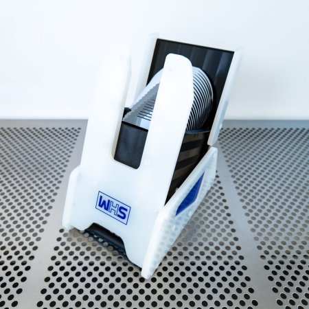
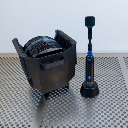
Automatic flat aligner (WHS-A1)
Automatic flat aligner (WHS-A1)
WHS-A1 Automatic Wafer Flat Aligner
Applications:
- Alignment - Wafer flat and notch aligners are used in the semiconductor industry to ensure that wafers are oriented correctly during various processes, such as lithography, deposition, and etching. The wafer has a notch or flat that corresponds to the orientation of the wafer's crystal lattice structure. This is critical because the orientation of the wafer affects the performance and functionality of the final semiconductor device.
- Lot integrity - Aligners are also used in the semiconductor industry to aid operators in performing lot integrity checks. By rotating the wafer scribe, which is the identification marking on the wafer's edge, to be visible to the operator, the operator can verify that the correct lot of wafers is being loaded into a production tool. This is an important step in preventing errors and ensuring consistent product quality.
- Edge inspection - Wafer flat and notch aligners are also used in the semiconductor industry to inspect wafers for edge defects. This macro inspection procedure is usually done under a light source and involves examining the edges of the wafer for any chips, cracks, or other imperfections. This is an important step in preventing wafer breakage during subsequent processing steps, as edge defects can weaken the wafer and cause it to break or fail. By using wafer flat and notch aligners to identify and inspect these defects, operators can take steps to prevent further processing of defective wafers and avoid costly production delays.
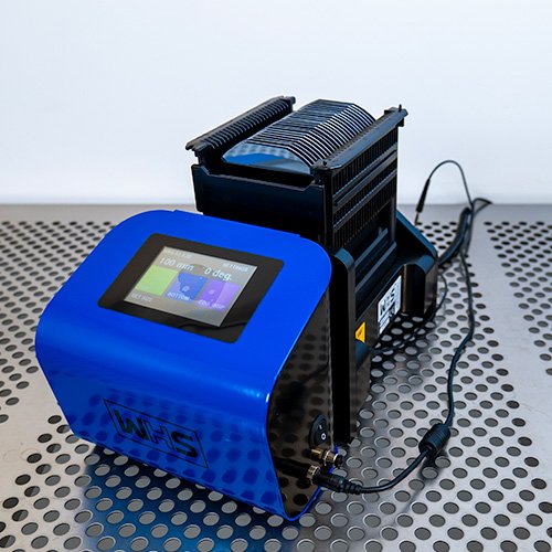
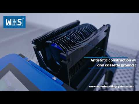
The WHS-A1 series from WHS is a state-of-the-art automatic flat aligner designed for precise wafer alignment across 76-, 100-, 125-, and 150-mm wafers, ensuring accuracy within ±1°. Built with cutting-edge technologies and ESD-safe materials, the WHS-A1 is ideal for handling advanced materials like InP, GaAs, GaN, and SiC, making it a perfect solution for today’s compound semiconductor industry. The system features a motorized stage for gentle wafer lifting, safeguarding the wafer edges and maximizing production yield.
The integrated touchscreen interface allows users to access multiple programs, including standard alignment, thin/compound wafer alignment, and edge-inspection modes. Designed for cleanroom environments, the WHS-A1 operates in ISO 3 (Class 1 FS209E) conditions, ensuring compliance with the strictest cleanliness and contamination control standards.
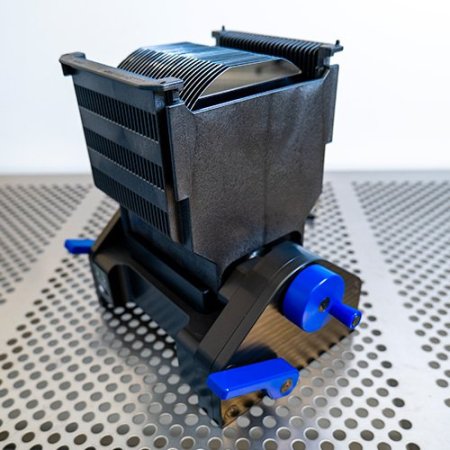
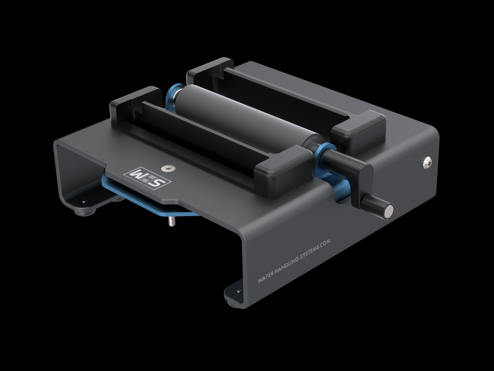
Quick-disconnect roller assemblies make the aligner easy to maintain, minimizing downtime, while compatibility with SEMI-compliant wafer cassettes provides seamless integration into existing processes.
Whether used for lot integrity, crystal orientation, or wafer edge inspection, the WHS-A1 is engineered to enhance operational efficiency and product quality. Manufactured in an ISO9001 and CE certified facility, the WHS-A1 aligns with the highest global standards for safety, performance, and reliability.

