Wafer Polishing Service

Wafer Polishing Service
Wafer Polishing Process - The Advantage of Polishing Film
Our process leverages the unique "flexibility" and "continuous cutting edge (grit) switching" of polishing films. This allows us to achieve:
- Low damage & high efficiency: A specialized in-house process that maintains wafer integrity while ensuring high polishing rates.
- Material versatility: By selecting specific films, we easily handle materials that are traditionally difficult to process using abrasive grinding or slurry methods.
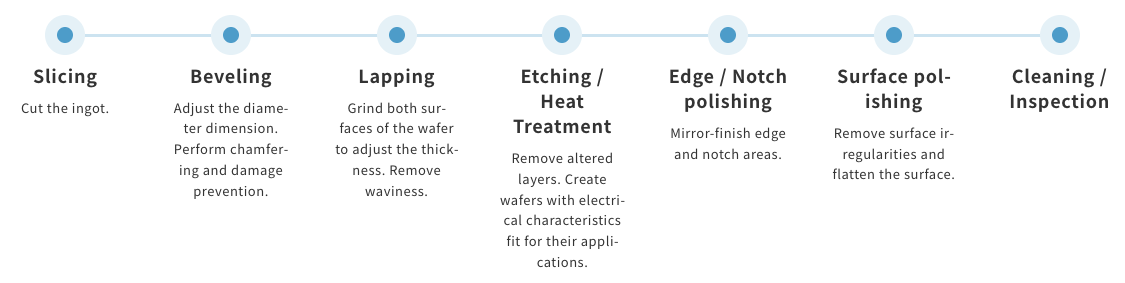
Key Applications: From Manufacturing to Post-Processing
Our services extend beyond initial wafer fabrication into critical semiconductor post-processing stages.
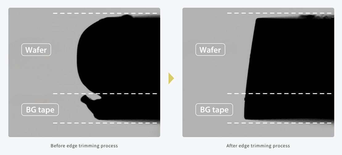
Featured Technology: Edge Trimming Process We have developed a proprietary "Edge Trimming Process" (Japanese Patent No. 4463326) specifically designed to prevent wafer damage during backgrinding (BG). This unique application is capable of removing the wafer edge and BG tape simultaneously.
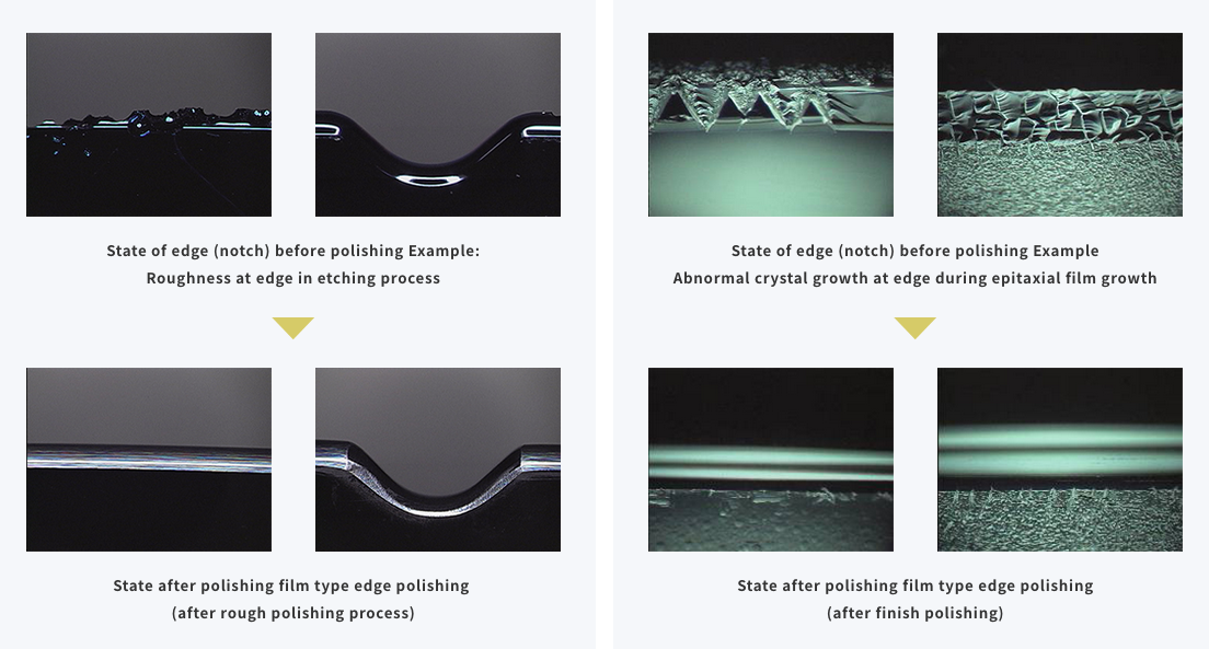
Technical Excellence in Edge Polishing and Chamfering
Mipox’s film based edge polishing service excels where traditional abrasive grinding and slurry methods struggle. Our technology is specifically engineered for difficult-to-machine materials, delivering customized edge profiles and surface roughness (Ra) with absolute precision.
Key Strengths of the Film Polishing Method
Unmatched Flexibility (High-Mix, Low-Volume): Unlike traditional grinding which requires unique stones for every edge profile, our method relies on software-driven "recipes." This allows us to modify edge shapes instantly, making it ideal for diverse product lines and small-scale production without the need for custom tooling.
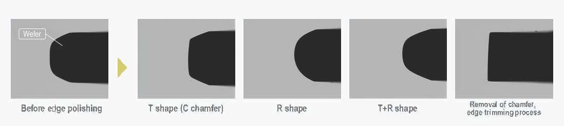
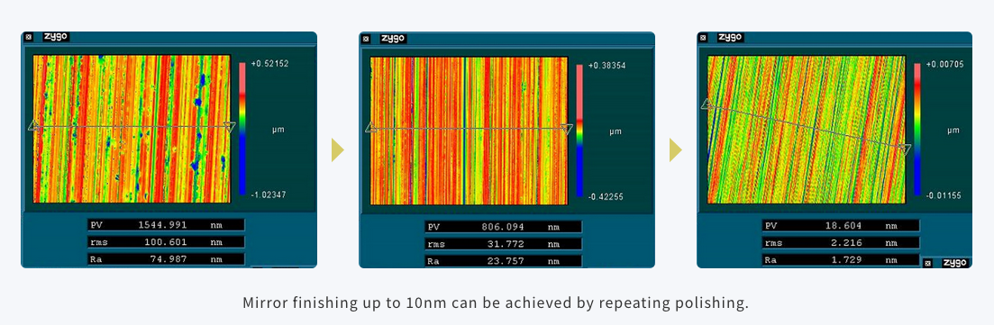
Precision Roughness Control: Surface roughness for both the edge and notch can be easily adjusted by simply selecting the appropriate polishing film grade.
Superior Wafer Integrity: Our method significantly reduces microscopic chipping and cracking compared to abrasive grinding. This makes it the preferred choice for delicate template substrates, such as GaN-on-Si.
Dry, Chemical-Free Process: Our edge polishing process does not utilize liquid chemicals (acids or alkalis). This eliminates the need for complex wafer cleaning stages and costly hazardous waste liquid treatment, streamlining your production line.
Superior Efficiency on Hard Materials: For challenging materials like SiC and GaN, our film-based technology achieves 3 to 5 times higher chamfering efficiency than traditional grinding methods.
Versatile Material Compatibility: We successfully process materials that are typically problematic for grinding, including resins and metals (such as Cu and Au membranes), ensuring a smooth finish without clogging or surface damage.
Edge Trimming
Preventing Edge Area Damage During Wafer Thinning Process.
General backgrinding (BG) situation without edge trimming
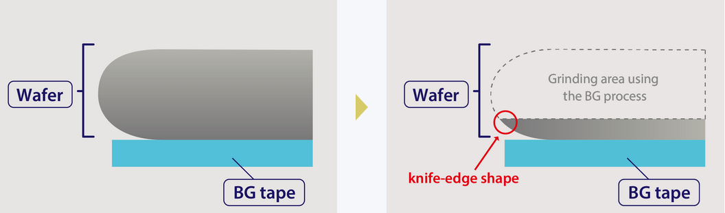
State of edge trimming using a polishing film method
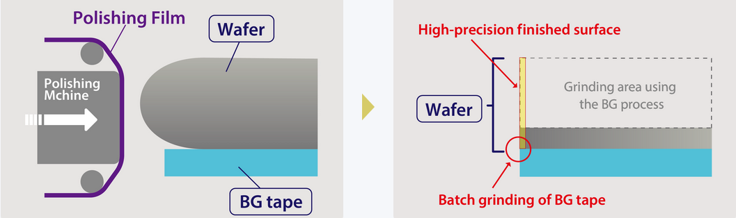
Mipox’s edge trimming service, using polishing film–type edge trimming, effectively improves yield in semiconductor wafer backgrinding (BG) processes. The service enables stable and consistent edge trimming regardless of the presence of resin films, metal layers (such as Cu or Au), or other materials in the wafer edge area. In addition, this process can be applied after BG tape attachment, allowing both the BG tape and the wafer edge to be trimmed simultaneously. As a result, edge trimming can be easily introduced without requiring changes to existing manufacturing processes.
Reclaimed Wafer Applications - Edge/Notch Membrane Removal
Mipox’s edge and notch polishing service, utilizing polishing film–type edge and notch polishing, efficiently removes unwanted films and defects while minimizing wafer diameter loss. Leveraging this capability, the service has been widely adopted with a strong track record in wafer reclamation applications within the reclaimed wafer market.
Even for wafers with carbon-based films where membrane removal by chemical etching is typically challenging or wafers in abnormal conditions with significant surface irregularities, this service can reliably restore proper edge quality.
In addition, the service supports reclamation polishing applications for large-diameter SiC wafers (8-inch), including both edge and notch areas.
Edge/Notch Cleaning Process
Mipox’s edge and notch polishing service, based on polishing film type edge polishing, addresses resin (adhesive) adhesion issues that can arise in edge areas during composite wafer manufacturing or when using high-bump backgrinding (BG) tape.
Unlike abrasive grinding or slurry-based methods, polishing film type processing is less susceptible to issues such as clogging caused by the physical properties of the target material. By applying a dedicated cleaning film, resin materials (including adhesives) adhering to edge and notch areas can be removed effectively.
This cleaning process, which is unique to the polishing film type method, contributes significantly to yield improvement, particularly in backgrinding (BG) processes.
Top Edge Polishing and Terrace Formation Polishing
For template wafers of GaNonSi (SiConSi9), GaNonSiC, and others, it is known that wafers are likely to be broken due to the difference in physical properties between the bulk and epitaxial layers. If some defects exist at the edges, the risk of damage to the entire wafer including the bulk increases, and even if that damage does not lead to breakage, the risk of the occurrence of fatal damage such as slip in the surface membrane (surface area formed by the heteroepitaxial growth) increases as well. Removing such defects in advance is very important.
Our top edge polishing (terrace formation polishing) using the polishing film type method reduces load on both the bulk and epitaxial layers and removes defects at the edges. Even a mirror surface can be achieved. This is one of the unique applications of the polishing film method that cannot be handled by abrasive grinding or slurry polishing methods.
Chip-Shaped and Non-Standard Size Wafer Chamfering
Our edge polishing service, utilizing polishing film type edge polishing, also supports chip-shaped (square) wafers used in research and development, as well as special small-diameter wafers with diameters of 1 inch or less, including half inch sizes.
Chip-shaped (square) wafers typically have sharp corners and edges, which can lead to breakage or edge chipping during processes such as planar polishing. Pre emptive chamfering to round these corners and edges is therefore critical to preventing damage and ensuring stable downstream processing.
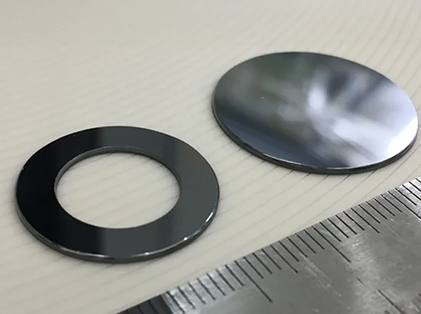
Half-inch wafers
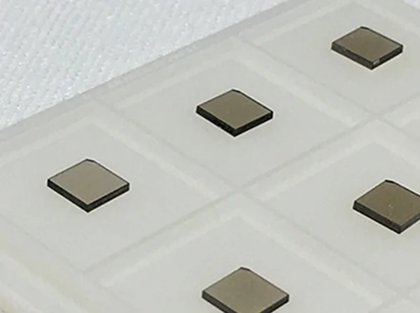
Diamond substrates (chips)
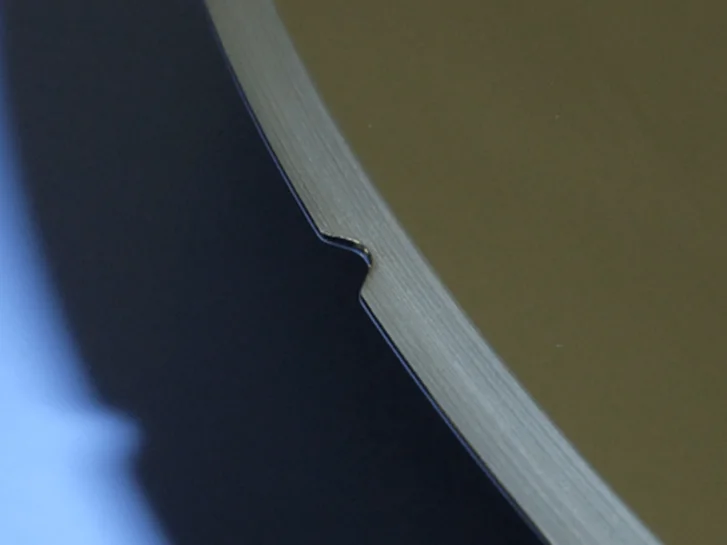
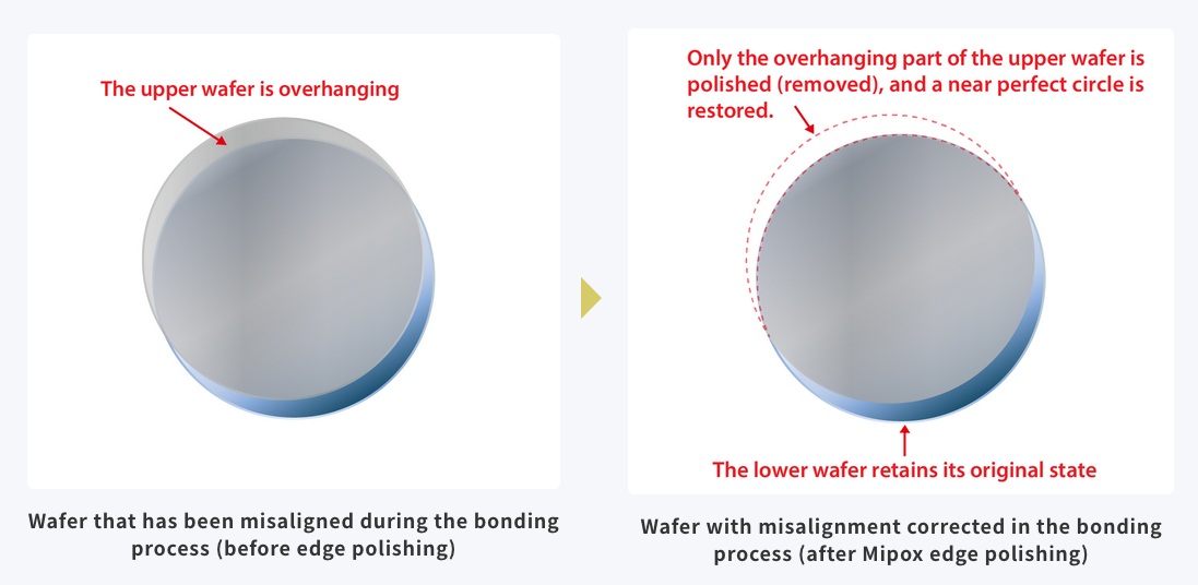
Wafer Bonding Alignment Correction
When two wafers of different materials are bonded, if misalignment occurs and causes edge protrusion, an almost perfect circular shape can be restored by polishing the relevant edge intensively.
Please request a quotation, and our sales managers will be pleased to support you in identifying the solution that best meets your requirements.

