Room Temperature Wafer Bonding

Room Temperature Wafer Bonding
Room temperature wafer bonding is a technique that joins dissimilar materials without the use of heat. By activating the wafer surfaces in an ultra-high-vacuum environment, strong and reliable bonds can be achieved without issues caused by thermal expansion, even when bonding different materials.
Mipox’s room temperature bonding service supports a wide range of material combinations, including silicon wafers, compound semiconductor wafers, oxide wafers, and ceramic wafers. The service is particularly suited to prototyping for power semiconductor devices, surface acoustic wave (SAW) filters, high-frequency devices, as well as various MEMS and LED applications.
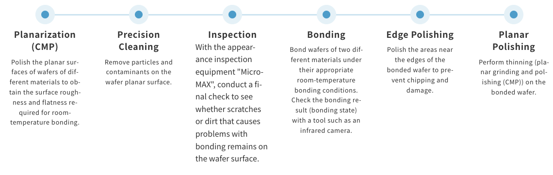
Wafer Room-Temperature Bonding Process Example
Requirements for Room-Temperature Wafer Bonding
Relationship Between Surface Roughness and Bonding Technology
Wafer bonding is an extremely sensitive process in which even microscopic surface irregularities or foreign particles measuring only a few nanometers can lead to defects such as void formation or insufficient bonding strength. For reliable bonding, wafer surfaces must be exceptionally smooth. Processes such as chemical mechanical polishing (CMP) typically require an arithmetic average surface roughness (Ra) of approximately 0.2 nm.
In addition, surface “roll-off” near the wafer edge can significantly degrade bonding quality. Therefore, advanced polishing technologies that effectively suppress edge roll-off are essential to achieving stable bonding performance.
Achieving Ultimate Surface Roughness
Mipox achieves high-quality room-temperature bonding through proprietary polishing technologies that produce ultra-smooth surface finishes. These techniques enable ultimate surface roughness levels even on materials traditionally regarded as difficult to polish, including compound semiconductor substrates (e.g., SiC and GaN), single-crystal diamond substrates, and polycrystalline sintered materials such as SiN and AlN.
This capability represents a significant advancement, extending room-temperature bonding applications to materials that were previously considered difficult or impractical to bond.
Ultra-High-Precision Alignment for Room-Temperature Bonding
Mipox’s room-temperature bonding systems utilize high-precision recognition of infrared (IR) transmission images and support ultra-high-accuracy alignment of ±0.2 μm. This precision is achieved through six-axis position control using piezoelectric actuators.
Conventional bonding alignment methods, which rely solely on planar alignment, are limited to an accuracy of approximately ±0.5 to 1.0 μm due to wafer misregistration upon contact. In contrast, Mipox’s ultra-high-precision alignment technology significantly exceeds these limitations, suppressing misalignment to within ±0.2 μm.
Please request a quotation, and our sales managers will be pleased to support you in identifying the solution that best meets your requirements.

