Planar Polishing (CMP) service
Planar Polishing (CMP) service
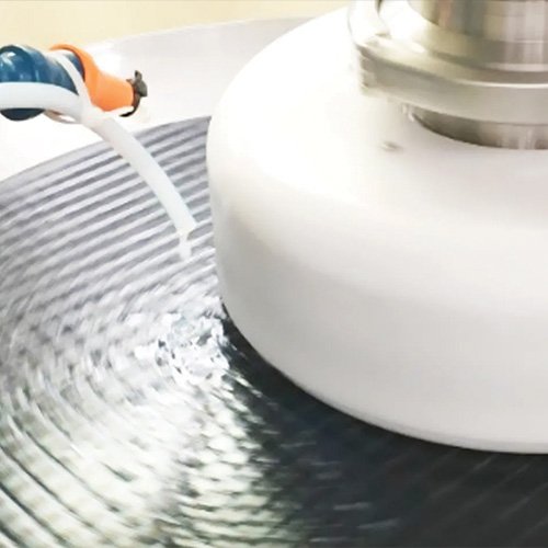
Mipox provides advanced planar polishing (CMP) solutions across a broad range of semiconductor and advanced material applications. Our capabilities extend from wafer and substrate planarization to CMP processing of insulating, metal, and resin films. We support substrate sizes ranging from small and chip-scale formats to SEMI-standard 12-inch wafers, offering exceptional flexibility for diverse production needs.
Broad Material Compatibility and Process Flexibility
Mipox responds precisely to customer requirements for material characteristics, surface roughness, thickness control (including warpage), and cleanliness. Our CMP services support both small-lot process and prototype development as well as stable medium-volume production.
Beyond CMP, we also offer precision cleaning and room-temperature bonding as integrated downstream processes, enabling streamlined and reliable manufacturing workflows.
Advanced Polishing for Diverse Materials
Our polishing services cover a wide variety of materials, including conventional semiconductor substrates such as single-crystal silicon and compound semiconductors, as well as composite, organic, and next-generation materials under development.
Key application areas include:
- Single-crystal and polycrystalline materials
- Film thickness control and roughness improvement
- Damascene (embedding) processes
- Wafer step elimination
- Hybrid bonding applications
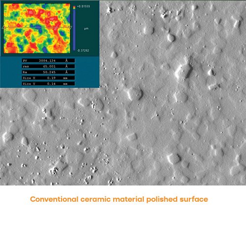
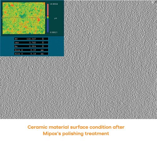
Mipox has particular expertise in ceramic materials, including sintered and polycrystalline bodies. These materials form a core strength of our polishing services, supported by a strong track record of technical innovation and proven results.
Ultra-High Precision Surface Finishing
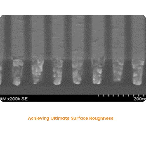
Mipox achieves ultra-low surface roughness even for materials traditionally considered difficult to polish, such as SiC, GaN, SiN, AlN, MgO/Al₂O₃, and other advanced ceramic substrates. Our in-house precision measurement systems—including ZYGO, AFM, and the Macro-Max visual inspection system—enable accurate and reliable surface evaluation.
By combining proprietary polishing film technology with specialized planar polishing equipment featuring oscillation and head-rotation mechanisms, we deliver processes ranging from high-rate material removal to mirror-level finishing. This enables wafer surfaces optimized for high-performance bonding applications.
Materials with Proven Track Records
Ceramic and Composite Materials SiC, AlN, Si₃N₄, Al₂O₃, YAG, PZT, MgAl₂O₄, and other sintered or polycrystalline ceramics.
Metal Films Cu, Al, Au, Pt, Ru, Mo, Ni, Ag, Ti, W, Fe-Ni alloys, Ni-P alloys, Cr, and other plated metal surfaces.
Enhanced Performance Through Grain Step Elimination
For ceramic and polycrystalline materials where planarization was once considered highly challenging, Mipox achieves superior surface precision through effective crystal grain step elimination. This results in reduced void formation, improved bonding strength, enhanced thermal performance, and improved optical characteristics in subsequent processes.
Please request a quotation, and our sales managers will be pleased to support you in identifying the solution that best meets your requirements.

