12" (300 mm) EFOSB
12" (300 mm) EFOSB
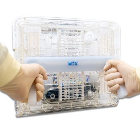
12" (300 mm) EFOSB 300-A eWB0531-A-ASSY-3-HFI-W
Type: Front Opening Shipping Box (FOSB)
Wafer slots: 25
First wafer position: 44 mm
Wafer spacing: 10 mm
Applications of FOSB and eFOSB in Semiconductor Manufacturing FOSB and eFOSB are utilized extensively in transporting FOSB wafers between manufacturing facilities, with critical applications in:
- Wafer Fabrication: Ensuring the protection of wafers during various fabrication stages.
- Inspection and Testing: Securely transporting wafers to testing facilities, preventing contamination.
- Assembly and Packaging: Guaranteeing that wafers arrive at assembly lines in immaculate condition.
- Long-Distance Transport: Offering robust protection for wafers during international transit.
- Storage: Serving as secure storage solutions for wafers, shielding them from environmental factors.
Introduction to FOSB and eFOSB Technology The Front Opening Shipping Box (FOSB) is essential in semiconductor manufacturing, serving as a vital semiconductor wafer carrier.
ePAK's eFOSB, an advanced version of FOSB, enhances this technology to cater specifically to the needs of FOSB wafer transportation. These systems are designed to function as more than shipping boxes; they serve as comprehensive solutions for maintaining wafer integrity and cleanliness, particularly in cleanroom settings.
Evolution and Design of FOSB and eFOSB, as clean cassette solutions, have revolutionized wafer transport. Adhering to industry standards, they ensure a contamination-free environment, crucial for the protection of semiconductor wafers. eFOSB, in particular, extends the capabilities of standard FOSB design, ensuring seamless integration into semiconductor manufacturing workflows and minimizing contamination risks. Role of FOSB and eFOSB as Semiconductor Wafer Carriers FOSB and eFOSB, as semiconductor wafer carriers, offer substantial benefits for the safe transportation and storage of FOSB wafers, including the commonly used 300 mm wafer sizes.
These systems ensure isolation from external contaminants during transportation and storage, maintaining the high standards required for semiconductor components. Future Outlook for FOSB and eFOSB The future of FOSB and eFOSB technologies in the semiconductor industry is set to be increasingly significant.
Anticipated advancements are expected to enhance compatibility with larger wafer sizes and new semiconductor materials. The integration of smart technologies for tracking and condition monitoring within FOSB and eFOSB will likely further optimize semiconductor manufacturing processes.


